
Best Method for Producing a Printed Circuit Board Prototype
The design and production of a printed circuit board prototype is an essential step in the process of developing a finished electronic device. The prototype will allow designers to test the function of the device, identify any errors and make necessary adjustments before full-scale production.
The prototyping phase enables designers to make changes in the physical dimensions and layout of the circuit boards, as well as the materials and components used in manufacturing. This flexibility in a prototype’s construction offers significant cost savings, as it prevents costly mistakes and unnecessary production delays that could occur during direct mass production.
printed circuit board prototype fabrication methods use subtractive and additive processes to create the desired patterns of conductive pathways on the substrate. Subtractive methods include chemical etching, where unwanted copper is removed from the surface of the substrate using a special solution, leaving behind the desired circuit traces. Additive methods are used for the creation of more complex multi-layer PCBs. These are more common in advanced electronics and mobile devices like smartphones, and require the highest degree of precision for successful operation.
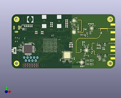
What is the Best Method for Producing a Printed Circuit Board Prototype?
To create a prototype, the designer will first assemble a bill of materials (BOM) that includes all the components that will be required for the final product. This step is important because the CM will need to know which components to order in order to fabricate the prototype according to the OEM’s design specifications.
When the BOM has been compiled, the CM will submit the file to the appropriate printer for prototyping. The CAD software used by the CM will need to match the same file format that the OEM used for the original design, as this will ensure accurate transmission of data throughout the entire prototyping process.
The resulting prototype will be composed of a base, known as the substrate, which is often made of fiberglass, but can also be made of other durable and lightweight materials such as polyimide or metal-core. This base layer acts as the core of the circuit board and provides the strength and rigidity needed for a successful outcome.
Depending on the design and intended final product, the next layer may be copper foil or a solid-on copper coating. The copper layer carries electrical signals from one end of the board to the other, much like the nervous system carries impulses from the brain to the muscles.
Once the copper layers have been properly plated, the traces are then drilled in the places where the component pins will be attached. A hole size must be selected that is compatible with the component leads and can accommodate the size of the solder paste to be used. Then, the components are placed on the board and soldered to their respective connections.
Once the components have been placed and soldered, the resulting prototype will undergo several quality checks to ensure that it meets the specifications of the intended final product. These quality tests will usually include a visual inspection and electrical testing.



+ There are no comments
Add yours